- 您现在的位置:买卖IC网 > Sheet目录1243 > SI5321-EVB (Silicon Laboratories Inc)BOARD EVALUATION FOR SI5321
�� �
�
�Si5321-EVB�
�and� a� 0.1� μ� F� capacitor,� such� that� the� positive� and�
�negative� inputs� of� the� differential� pair� each� see� a� 50� ?�
�termination� to� “ac� ground,”� and� the� line-to-line�
�termination� impedance� is� 100� ?� .�
�For� single-ended� operation,� supply� a� signal� to� one� of�
�the� differential� inputs� (usually� the� positive� input).� The�
�other� input� should� be� shorted� to� ground� using� an� SMA�
�shorting� plug.� The� on-board� termination� circuit� provides�
�a� 50� ?� termination� to� ac-ground� for� each� leg� of� the�
�differential� pair.�
�Differential� Clock� Output� Signals�
�The� differential� clock� outputs� from� the� Si5321� device�
�are� routed� to� the� perimeter� of� the� circuit� board� using�
�50� ?� transmission� line� structures.� The� capacitors� that�
�provide� ac-coupling� are� located� near� the� clock� output�
�SMA� connectors.�
�Internal� Regulator� Compensation�
�The� Si5321-EVB� contains� pad� locations� for� a� resistor�
�and� a� capacitor� between� the� VDD25� node� and� ground.�
�The� resistor� pads� are� populated� with� a� 0� ?� resistor.� The�
�capacitor� pads� are� populated� with� a� low� ESR� 33� μ� F�
�tantalum� capacitor.� This� is� the� suggested� compensation�
�circuit� for� Si5321� devices.�
�There� are� two� considerations� for� selecting� this�
�combination� of� compensation� resistor� and� capacitor.�
�First,� is� the� stability� of� the� regulator.� The� second� is� noise�
�filtering.�
�The� acceptable� range� for� the� time� constant� at� this� node�
�is� 15� μ� s� to� 50� μ� s.� The� capacitor� used� on� the� board� is� a�
�33� μ� F� capacitor� with� an� ESR� of� .8� ?� .� This� yields� a� time�
�constant� of� 26.4� μ� s.� The� designer� could� decide� to� use� a�
�330� μ� F� capacitor� with� an� ESR� of� .15� ?� .� This� yields� a�
�time� constant� of� 49.5� μ� s.� Each� of� these� cases� provide� a�
�compensation� circuit� that� makes� the� output� of� the�
�regulator� stable.�
�The� second� issue� is� noise� filtering.� For� this,� more�
�capacitance� is� usually� better.� For� the� two� cases�
�described� above,� the� 330� μ� F� case� provides� greater�
�noise� filtering.� However,� the� large� case� size� of� the�
�330� μ� F� capacitor� might� make� it� impractical� for� many�
�applications.� The� Si5321� device� is� specified� with� the�
�33� μ� F� cap.�
�Default� Jumper� Settings�
�The� default� jumper� settings� for� the� Si5321-EVB� board�
�are� given� in� Table� 1.� These� settings� configure� the� board�
�for� operation� from� a� 3.3� V� supply.�
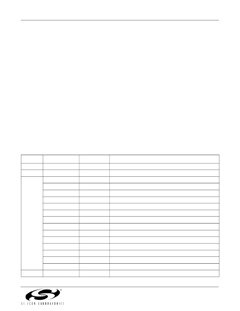
�Table� 1.� Si5321-EVB� Assembly� Rev� B-01� Default� Jumper/Switch� Settings�
�Location�
�JP6�
�JP1�
�JP5�
�JP7�
�Signal�
�VSEL33�
�VDD33�
�VALTIME�
�FEC[0]�
�FEC[1]�
�FEC[2]�
�BWSEL[0]�
�BWSEL[1]�
�INFRQSEL[0]�
�INFRQSEL[1]�
�INFRQSEL[2]�
�FRQSEL[0]�
�FRQSEL[1]�
�FRQSEL[2]�
�BWBOOST�
�FXDDELAY�
�LED� ENABLE�
�State�
�1�
�Open�
�0�
�0�
�0�
�0�
�0�
�1�
�1�
�0�
�0�
�1�
�1�
�0�
�1�
�0�
�On�
�Rev.� 0.4�
�Notes�
�Internal� Regulator� enabled�
�3.3� V� plane� not� connected� to� 2.5� V� plane�
�100� ms� Validation� Time�
�No� FEC� scaling�
�No� FEC� scaling�
�No� FEC� scaling�
�Loop� Filter� Bandwidth� =� 800� Hz�
�Loop� Filter� Bandwidth� =� 800� Hz�
�Clock� IN� =� 19.44� MHz�
�Clock� IN� =� 19.44� MHz�
�Clock� IN� =� 19.44� MHz�
�Clock� Out� =� 622.08� MHz�
�Clock� Out� =� 622.08� MHz�
�Clock� Out� =� 622.08� MHz�
�Selected� bandwidth� not� doubled�
�Fixed� Delay� disabled�
�LED� Indicators� enabled�
�3�
�发布紧急采购,3分钟左右您将得到回复。
相关PDF资料
SI5364-EVB
BOARD EVALUATION FOR SI5364
SI5XX-PROG-EVB
KIT EVALUATION FOR SI5XX
SI84XXCOM-RD
KIT EVAL FOR SI84XXCOM
SILICON-EXPLORER II
SOFTWARE ANALYSIS EXPLORER LOGIC
SILINKPS-EVB
DAUGHTER CARD PROSLIC PS
SKP16C26A
DEV EVALUATION KIT M16C/26A
SKP32C85-100-CL
DEV EVALUATION KIT M32C/85 100PN
SKP8CMINI-13
BOARD DEV EVALUATION FOR R8C/13
相关代理商/技术参数
SI5321-F-BC
功能描述:时钟合成器/抖动清除器 FOR NEW DESIGNS
RoHS:否 制造商:Skyworks Solutions, Inc. 输出端数量: 输出电平: 最大输出频率: 输入电平: 最大输入频率:6.1 GHz 电源电压-最大:3.3 V 电源电压-最小:2.7 V 封装 / 箱体:TSSOP-28 封装:Reel
SI5321-G-BC
功能描述:时钟发生器及支持产品 SONET/SDH Precision Clock 19 to 2500MHz RoHS:否 制造商:Silicon Labs 类型:Clock Generators 最大输入频率:14.318 MHz 最大输出频率:166 MHz 输出端数量:16 占空比 - 最大:55 % 工作电源电压:3.3 V 工作电源电流:1 mA 最大工作温度:+ 85 C 安装风格:SMD/SMT 封装 / 箱体:QFN-56
SI5321-G-XC2
制造商:Silicon Laboratories Inc 功能描述:
Si5321-H-BL
功能描述:时钟发生器及支持产品 SONET/SDH Precisn Clock Multiplr RoHS:否 制造商:Silicon Labs 类型:Clock Generators 最大输入频率:14.318 MHz 最大输出频率:166 MHz 输出端数量:16 占空比 - 最大:55 % 工作电源电压:3.3 V 工作电源电流:1 mA 最大工作温度:+ 85 C 安装风格:SMD/SMT 封装 / 箱体:QFN-56
Si5321-H-GL
功能描述:时钟发生器及支持产品 SONET/SDH Precisn Clock Multiplr RoHS:否 制造商:Silicon Labs 类型:Clock Generators 最大输入频率:14.318 MHz 最大输出频率:166 MHz 输出端数量:16 占空比 - 最大:55 % 工作电源电压:3.3 V 工作电源电流:1 mA 最大工作温度:+ 85 C 安装风格:SMD/SMT 封装 / 箱体:QFN-56
SI5321-H-ZL2
制造商:Silicon Laboratories Inc 功能描述:
Si5321-XLNX-DC
功能描述:子卡和OEM板 Silabs/Xilinx Ref Design RoHS:否 制造商:BeagleBoard by CircuitCo 产品:BeagleBone LCD4 Boards 用于:BeagleBone - BB-Bone - Open Source Development Kit
SI5322
制造商:SILABS 制造商全称:SILABS 功能描述:Pin-Controlled 1_710 MHz Jitter Cleaning Clock